FPGA Oscilloscope
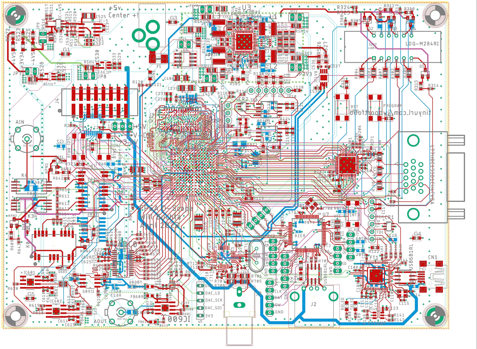
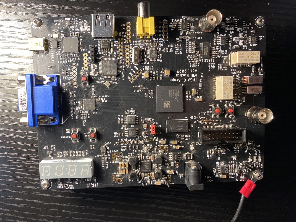
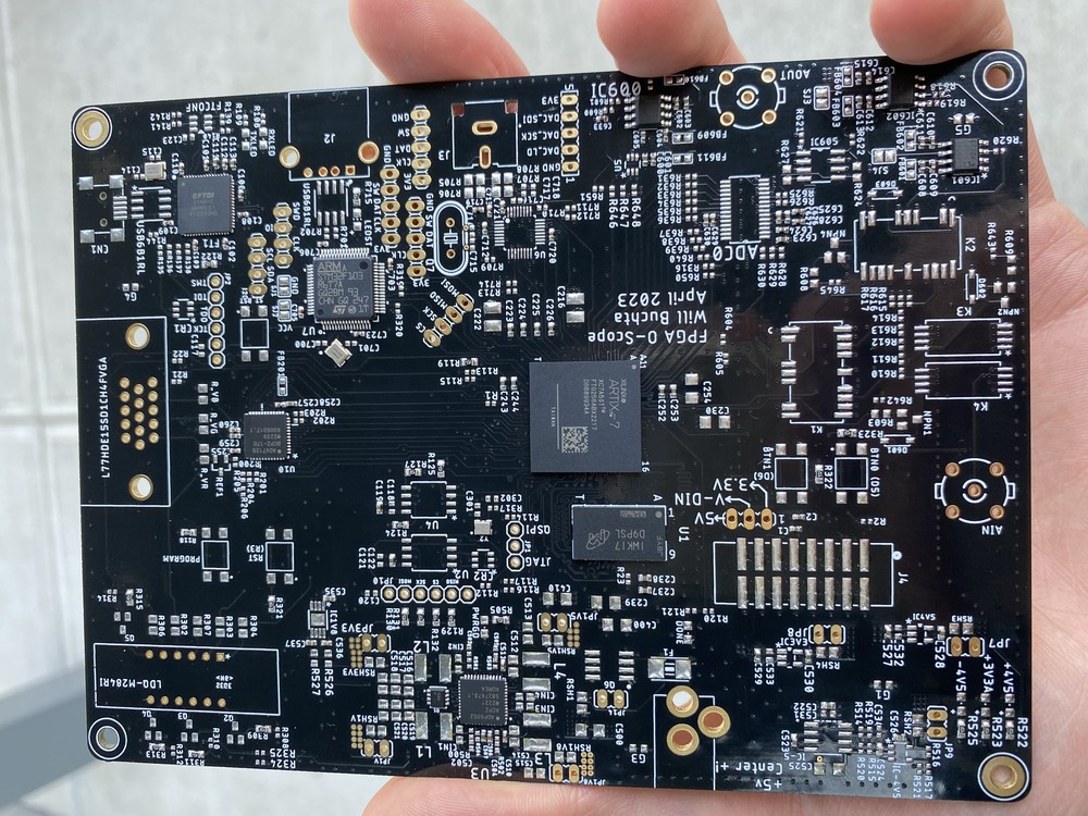
The completed PCB layout for an Oscilloscope powered by an FPGA. Not shown: GND or PWR layers.
A shift in the currents
Once I had a few PCB designs under my belt, I felt it was time to make something that would help me learn a complex topic. I also felt that I should "graduate" from Tesla Coils - don't get me wrong, I think they're great, obviously, but I knew it would be beneficial to focus my skills on something that would get the eyes of those in industry.
Up to this point, I had completed most of the analog EE courses at WPI and spent a summer with Analog Devices working on Op-Amps. Wanting to expand into the digital realm ("The Dark Side" as they called it at Analog), I set my sights on FPGAs. Unfortunately, I was at the mercy of the global supply chain and everything was out of stock at the height of the chip shortage.
Objectives
Once I saw that low range FPGAs were back in stock and mostly affordable, I began scoping out the project. FPGAs have a wide range of possible applications, so I needed to decide what to make. Based on my skill set at the time, I decided that making an oscilloscope would be a good balance between difficulty, usefulness, and coolness.
As this was going to be the most complicated project I worked on to-date, I understood that the chance of me overlooking a design nuance was high. Therefore, I set a "ceiling" on what features to include, and how advanced those features could be. For example, the ADC I chose has a simple parallel interface, and matches the speed of a mid-range scope from the early 2000s. I prioritized making something functional over making the most advanced artix dev board the world has ever seen. Not to mention that I already had plenty of work on my hands. It was also my first board with QFN and BGA packages - I figured it was worth it to use an assembly house to at least place the most complex parts, allowing me to use more industry standard packages. With that said, the board has the following features:
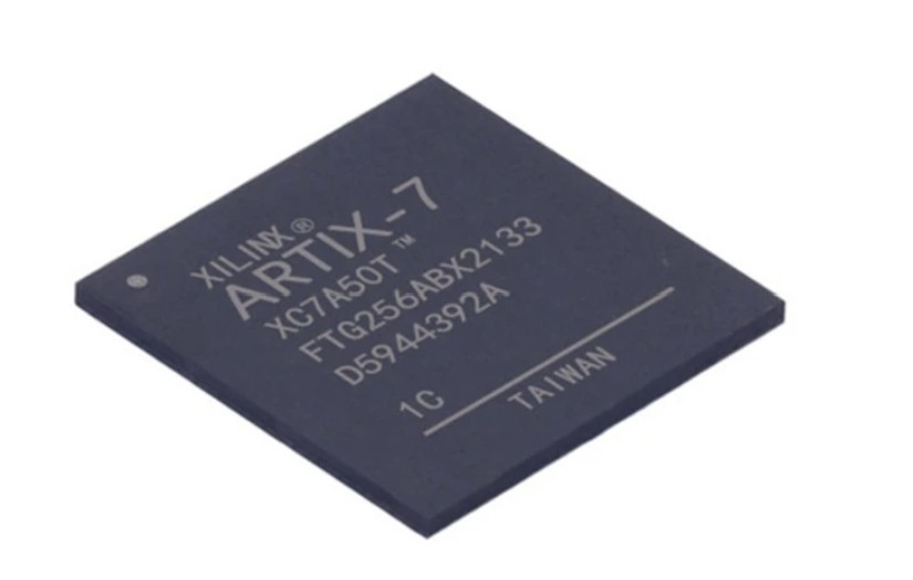
- FPGA: XC7A50t (Artix 7 FPGA in a 1mm, 256-pin BGA)
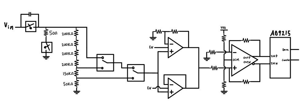
- ADC: AD9215 (105MSPS, 10-bit, 5-stage pipelined A/D, TSSOP-28)
- Digital probe: 8 FPGA pins broken out for digital sampling
- Memory: MT41J128M16JT (256MB DDR3, 16 bit interface, 96-pin BGA)
- Video DAC: ADV7125 (24 bit current DAC used for VGA output)
- USB Bridge: FT2232HQ
- DAC: LTC2630 12-bit, serial interface
- 4-digit 7-segment display
- STM32 MCU for keyboard/mouse interface
- Composite video decoder just for fun
Outcomes
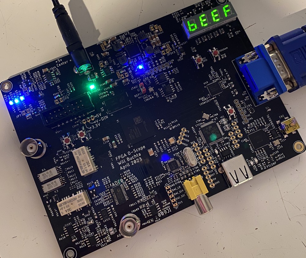
Long story short, I ended up using an 8-layer PCB stackup from PCBWay, and had some partial assembly done by Liberty Engineering in Newton, MA. I had them place the parts I had no chance of soldering myself, and any components that had a substantial quantity such as 0.1uF capacitors. The rest was hand soldered by me, deleting an entire weekend.
Part way through the project, I decided to try and get course credit for my work. Professor Schaumont of WPI agreed to sponsor an Independent Study, easing my schedule as a double major and allowing my work to count towards my undergrad degree.
Please see the following document for more details about the project. If loading does not work (which is common on mobile), click here.
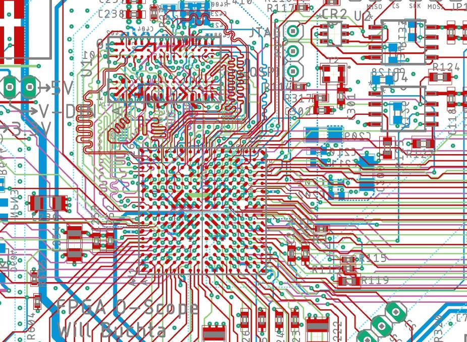
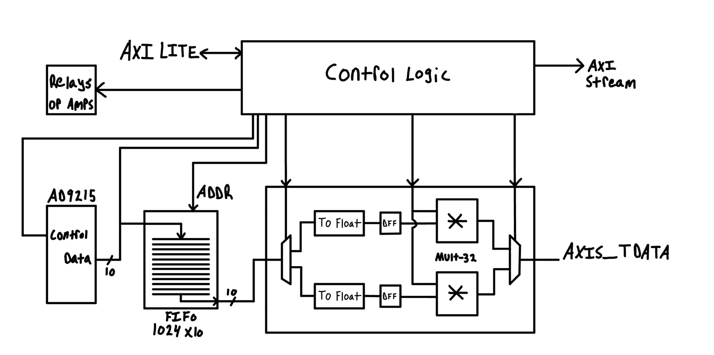
As mentioned in the report, the project's current status is stuck at debugging data transfer from the ADC to DDR memory. Turns out this stuff is challenging!! The hardest part of the PCB design was the FPGA and DDR routing, while the hardest part of the software/HDL portion has been designing a functional digital system. It really makes me appreciate the work done by engineers at companies like Keysight, who made a 128GSPS scope with custom silicon.
The final schematic for the PCB can be found here.